


+86 185 7539 8899
An ESD protection diode is a component that rapidly conducts to reduce impedance when high-voltage pulses caused by electrostatic discharge (ESD) and other factors enter the circuit, thereby protecting the IC. This article introduces the working principle of the most commonly used ESD protection diode in this application.
At present, Internet of Things (IoT) devices, smart phones and other mobile devices are everywhere. With the frequent plugging and unplugging of USB, Lightning interfaces and other cables, these electronic devices are highly vulnerable to ESD shocks. Therefore, providing system-level ESD protection is more important than ever. ESD protection diodes are a well-known solution for electrostatic protection. The following introduces the working principle of ESD protection diodes.
ESD protection diodes utilize Zener breakdown * of pn junction diodes. As shown in the following figure, the pn junction diode conducts in the forward direction at approximately 0.7V and begins to conduct in the reverse direction at the Zener voltage (VZ), which varies with the diode. ESD protection diodes utilize the reverse bias characteristic of pn junctions.
As shown in Figure 1, the ESD protection diode is connected along the signal line or control line between the protected device (DUP) and the connector exposed to the ESD environment. In addition to Zener voltage (VZ), ESD protection diodes also have reverse bias characteristics, known as reverse peak operating voltage (VRWM). VZ is the minimum voltage at which an ESD protection diode is on, while VRWM is the maximum voltage at which it remains off. The ESD protection diode is always reverse-biased connected. Let VIN be the voltage of the signal line connected to the ESD protection diode. Then, when GND < VIN ≤ VRWM, the diode does not conduct.
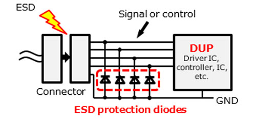
Figure 1: Example of ESD protection diode insertion
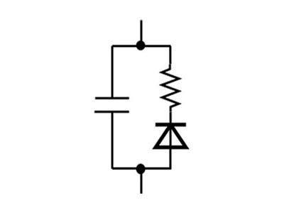
Figure 2: Equivalent circuit of ESD protection diode
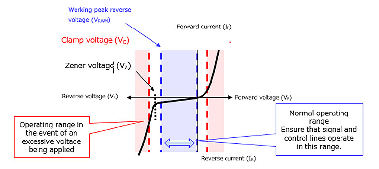
Figure 3: Current-voltage curve and operating range of pn junction diode
Suppose ESD surges enter the system during normal operation.
During normal operation, the ESD protection diode remains off.
In this state, as the pn junction forms a depletion region, they act as capacitors, and the total capacitance is CT. CT varies depending on the diode and can be as low as 0.2 pF.
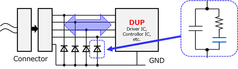
Figure 4: Working principle and equivalent circuit under normal conditions
When ESD or other overvoltage is applied, the ESD protection diode conducts.
At this point, the ESD protection diode can be regarded as composed of a voltage source and a resistor with a tiny dynamic resistance (RDYN). When the voltage source is forward-biased relative to the diode, it provides the forward voltage (VF). When the voltage source is reverse-biased relative to the diode, it provides the clamping voltage (VC), which is the Zener voltage defined in the high current region.
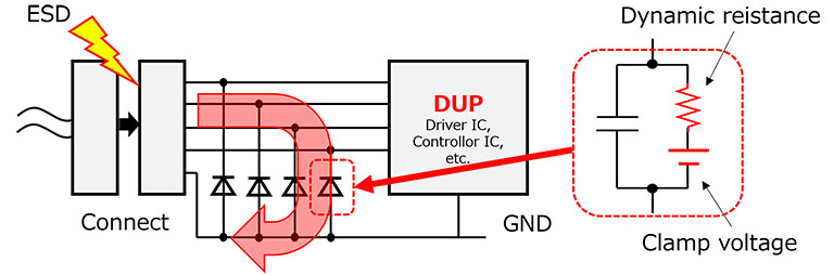
Figure 5: Working principle and equivalent circuit under ESD surge conditions
In the off state, the ESD protection diode acts as a capacitor, and in the on state, it serves as a voltage source and a micro-resistor. When choosing ESD protection diodes for high-frequency circuits, attention should also be paid to the total capacitance.
Now, let's consider the tiny dynamic resistance (RDYN) of the ESD protection diode when it is conducting.
The following figure shows the simplest circuit configuration, indicating the flow of current in the circuit when the voltage is too high (such as ESD surge voltage).
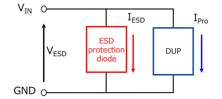
Figure 6: Simple circuit configuration under ESD surge conditions
The ESD protection circuit is connected in parallel with the DUP as shown above. Therefore, the ESD surge voltage (VESD) applied across the ESD protection diode is also applied across the DUP. In fact, due to the parasitic inductance and capacitance of the circuit board traces, the voltage and time applied to the ESD protection diode and DUP are slightly different. The current flowing into the DUP (IPro) is affected by the state of its internal active circuit and depends on the VESD.
Therefore, the most important aspect of protecting DUP is to reduce VESD, which depends on the clamping voltage of the ESD protection diode.
Figure 5 shows the equivalent circuit of the ESD protection diode in the on state, which includes a dynamic resistor connected in series with the clamped voltage source. This means that as IESD increases, a voltage drop occurs in the clamping voltage.
ESD is the sudden discharge of static electricity when two charged objects come into contact with each other. For detailed information, please refer to the FAQ "What is Electrostatic Discharge (ESD)?" "
What is electrostatic discharge (ESD)?
Just like a capacitor discharges, ESD releases an extremely high current immediately upon contact. For instance, the peak current of the ESD waveform specified in the ESD immunity test standard 61000-4-2 is as high as 30 A. Suppose the dynamic resistance of the ESD protection diode is 0.5 Ω. Then, the peak current of ESD will cause a 15V instantaneous voltage drop.
Therefore, in order to enhance the protection performance, considering the resulting voltage drop, it is important to select an ESD protection diode that not only has a low clamping voltage but also a low dynamic resistance.
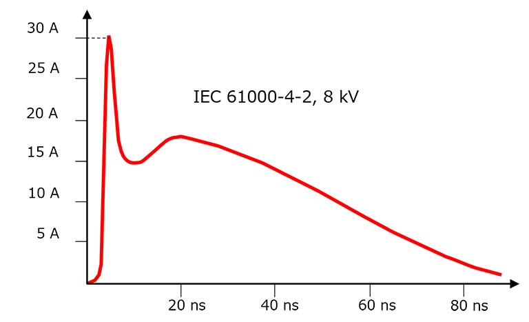
Figure 7: ESD Test Waveform Example (IEC 61000-4-2)
Figure 7 shows that ESD is a high-frequency pulse applied instantaneously. Therefore, attention should be paid to the position and routing of the ESD protection diode to achieve the best performance